Executive Overview & Market Positioning
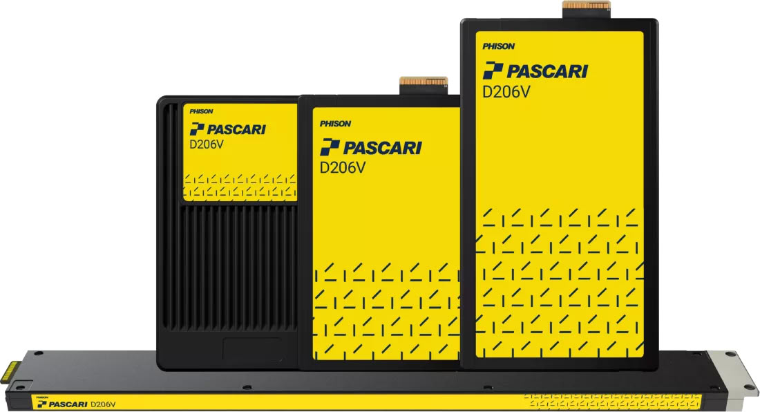
Phison has introduced a computational enterprise solid-state drive (SSD) architecture featuring an integrated Neural Processing Unit (NPU) and 64 GB of onboard memory. Unveiled at the Supercomputing 2026 (SC26) exhibition in Chicago, this hardware evolution addresses the fundamental I/O bottlenecks of modern artificial intelligence workloads. By shifting inferencing operations directly to the storage tier, the design aims to minimize host-to-device data transfers for large-scale language models and heavy data analytics frameworks.
The industry-wide race to integrate localized AI processing into peripheral hardware has driven controller manufacturers to rethink traditional NVMe topologies. Phison’s approach bypasses conventional PCIe bus saturation by executing parallel dataset scans and in-situ processing. By transmitting only finalized inferences or filtered subsets rather than raw multi-terabyte datasets across the host interface, the architecture significantly reduces latency and conserves host CPU cycles. While still in the proof-of-concept phase, this design signals a major paradigm shift toward intelligent, self-contained storage nodes.
Empirical Benchmark Matrix
Quantifying the efficiency of computational storage requires evaluating memory bandwidth, compute capability, and framework compatibility against standard host-bound baseline SSD architectures. Phison’s prototype pairs its dedicated NPU with high-speed local memory capable of sustaining 130 GB/s, while supporting standard AI toolsets including PyTorch, vLLM, OpenVINO, and llama.cpp. Notably, Phison utilizes DMIPS (Dhrystone Million Instructions Per Second) instead of the conventional TOPS metric to quantify NPU throughput, reflecting a specialized compute profile optimized for data movement and logical control.
| Hardware Parameter | Standard Enterprise NVMe Baseline | Phison NPU Computational SSD Prototype |
|---|---|---|
| Onboard Compute | Host CPU / GPU Dependent | Integrated Hardware NPU |
| Local Accelerator Memory | None (Host DRAM / VRAM Bottlenecked) | 64 GB Onboard Memory |
| Memory Bandwidth | Limited by PCIe Gen 5/6 Bus Width | 130 GB/s Local Bus Throughput |
| Framework Support | Host-Executed Only | Native PyTorch, vLLM, OpenVINO, llama.cpp |
| Data Transfer Efficiency | Baseline (Moves Full Dataset to Host) | 10x–100x Reduction (In-Situ Filtering) |
| Performance Metric | IOPS / GB/s Transfer Rate | DMIPS (Processor Control) & IOPS |
Thermal, Efficiency & Definitive Verdict
Implementing high-performance compute silicon directly on an enterprise storage PCB introduces severe thermal density and power dissipation challenges. Running an NPU alongside high-density NAND flash controllers will require robust active chassis cooling or specialized heatsink designs to prevent thermal throttling under sustained machine learning loads. Furthermore, missing architectural details—such as the host interface standard, exact controller model, and NAND flash type—leave key thermal-efficiency questions unanswered until silicon samples reach validation labs.
Ultimately, Phison’s computational SSD represents a forward-looking proof of concept that addresses the unsustainable bandwidth demands of modern AI pipelines. By reducing data transit overhead by a projected factor of 10 to 100, this architecture redefines the boundary between storage and compute. Enterprise architects should monitor its commercialization trajectory closely as a potential blueprint for next-generation distributed AI data centers.