Executive Summary & Market Positioning
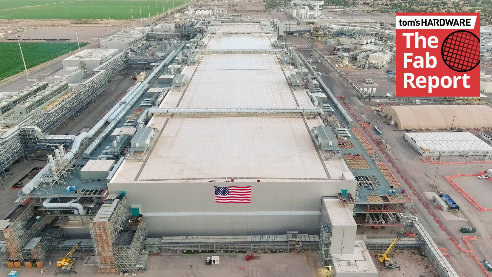
Intel Corporation has officially commenced the critical phase of production tool installation at its Fab 62 facility within the Ocotillo campus in Chandler, Arizona, keeping the massive Greenfield fab on track for operational readiness by late 2028. This infrastructure milestone is bolstered by tangible progress at the Ohio One manufacturing complex, where workers recently hoisted the first major structural truss. Together, these expansions underline Intel Foundry’s aggressive strategy to scale a sovereign, end-to-end U.S. manufacturing ecosystem capable of serving both internal product divisions and external enterprise design wins.
Positioned against a rapidly evolving global foundry landscape, Intel’s domestic push relies on an integrated model that spans advanced logic research, photomask fabrication, and sophisticated 3D packaging. While rival pure-play foundries continue to build localized wafer fabrication capacities, they often lack the localized process R&D and captive mask-shop infrastructure that Intel is actively deploying across Arizona, Oregon, New Mexico, and California. By combining these nodes with early commercial insertion of High-Na EUV lithography, Intel aims to secure a structural advantage in process density, supply chain resilience, and time-to-market execution.
Core Architectural & Technological Innovations
At the technological core of Intel's current scaling phase is the deployment of High-Numerical Aperture (High-NA) Extreme Ultraviolet (EUV) lithography. Having installed the industry's first commercial High-NA scanner at its D1X development fab in Hillsboro, Oregon, Intel has successfully transitioned the tool into high-volume manufacturing (HVM) workflows, utilizing it to pattern select tiles for upcoming client architectures such as the Panther Lake CPU family. While early deployment phases primarily replicate the design rule targets of mature Low-NA EUV infrastructure, this empirical trial run provides Intel's engineering teams with invaluable operational data regarding pellicle handling, stochastic defect reduction, and overlay control.
Concurrently, the manufacturing roadmap for the newly tooled Fab 62 highlights strategic flexibility. Originally earmarked alongside Fab 52 for early 20nm-class (Intel 20A) and 1.8nm-class (Intel 18A) nodes, Fab 62 currently remains unassigned to a specific single process node. However, given the facility's modular cleanroom architecture and Intel's updated process cadence, Fab 62 is ideally positioned to absorb overflow Intel 18A, optimized 18A-P capacity, or transition directly into the forthcoming Intel 14A era. This infrastructural adaptability ensures that Intel can dynamically reallocate wafer starts based on customer demand and yield maturity.
Empirical Specifications & Benchmark Matrix
| Feature / Metric | Intel Foundry (U.S. Operations) | Competitor Baseline (Foundry Average) | Advantage / Implication |
|---|---|---|---|
| Lithography Technology | High-NA EUV (0.55 NA) & Low-NA EUV | Standard Low-NA EUV (0.33 NA) | Higher single-exposure resolution potential for sub-2nm nodes. |
| Domestic Photomask R&D | Captive Santa Clara Facility | Distributed / Outsourced Overseas | Complete control over proprietary IP security and mask turnaround times. |
| Advanced Packaging | EMIB, EMIB-T, Foveros, Foveros Omni | Standard 2.5D TSV / CoWoS equivalents | Diverse multi-die interconnect topologies spanning R&D to high-volume production. |
| Domestic Supply Chain | >4,500 U.S. Suppliers ($29B+ annual spend) | Fragmented regional ecosystems | Lower geopolitical exposure and tighter feedback loops between design and fab. |
Thermal, Efficiency & Real-World Ergonomics
Transitioning leading-edge nodes from paper to high-volume manufacturing fundamentally alters the thermal and electrical efficiency profiles of silicon architectures. The integration of backside power delivery—a hallmark of Intel's 18A and subsequent nodes—decouples power delivery routing from signal interconnects on the front side of the wafer. This architectural pivot drastically reduces IR drop, curtails voltage droop during transient spikes, and allows dense server and client compute tiles to sustain higher boost frequencies within tightly constrained thermal design power (TDP) envelopes.
Furthermore, the synergies between advanced packaging methodologies implemented across New Mexico and Oregon enable tighter thermal dissipation pathways in heterogeneous multi-chiplet layouts. By leveraging technologies such as EMIB-T and Foveros, Intel minimizes thermal interface resistance between compute, I/O, and memory tiles. This ensures that massive parallel workloads executed on advanced nodes maintain lower junction temperatures ($T_j$), directly translating into superior sustained multi-core performance, improved energy efficiency ratios (perf/Watt), and enhanced long-term silicon reliability in enterprise datacenters.
The Definitive Verdict
Intel’s latest operational updates demonstrate that its ambitious manufacturing transformation is moving past the foundational civil engineering phase and entering active tool-in execution. The installation of production hardware at Fab 62, combined with pioneering high-volume deployments of High-NA EUV and localized photomask production, provides a compelling blueprint for sovereign semiconductor manufacturing. While questions remain regarding the exact node assignment for Fab 62 and the finalized operational timeline for Ohio One, Intel’s unmatched domestic depth—spanning from raw materials and R&D to advanced packaging—positions the company as a formidable, highly resilient engine of hardware innovation.