Executive Overview & Market Positioning
Thermal dissipation remains the primary physical bottleneck constraining high-density semiconductor performance, particularly within enterprise AI accelerators and GPU architectures exceeding 700W per square centimeter. Traditional metallic thermal interface materials and copper heat sinks are rapidly approaching their fundamental thermodynamic limits. To circumvent these boundary-layer constraints, the semiconductor packaging industry is aggressively evaluating ultrawide bandgap materials. Diamond possesses an exceptional thermal conductivity profile—demonstrating empirical metrics roughly five times greater than high-purity copper—while retaining robust electrical insulation properties.
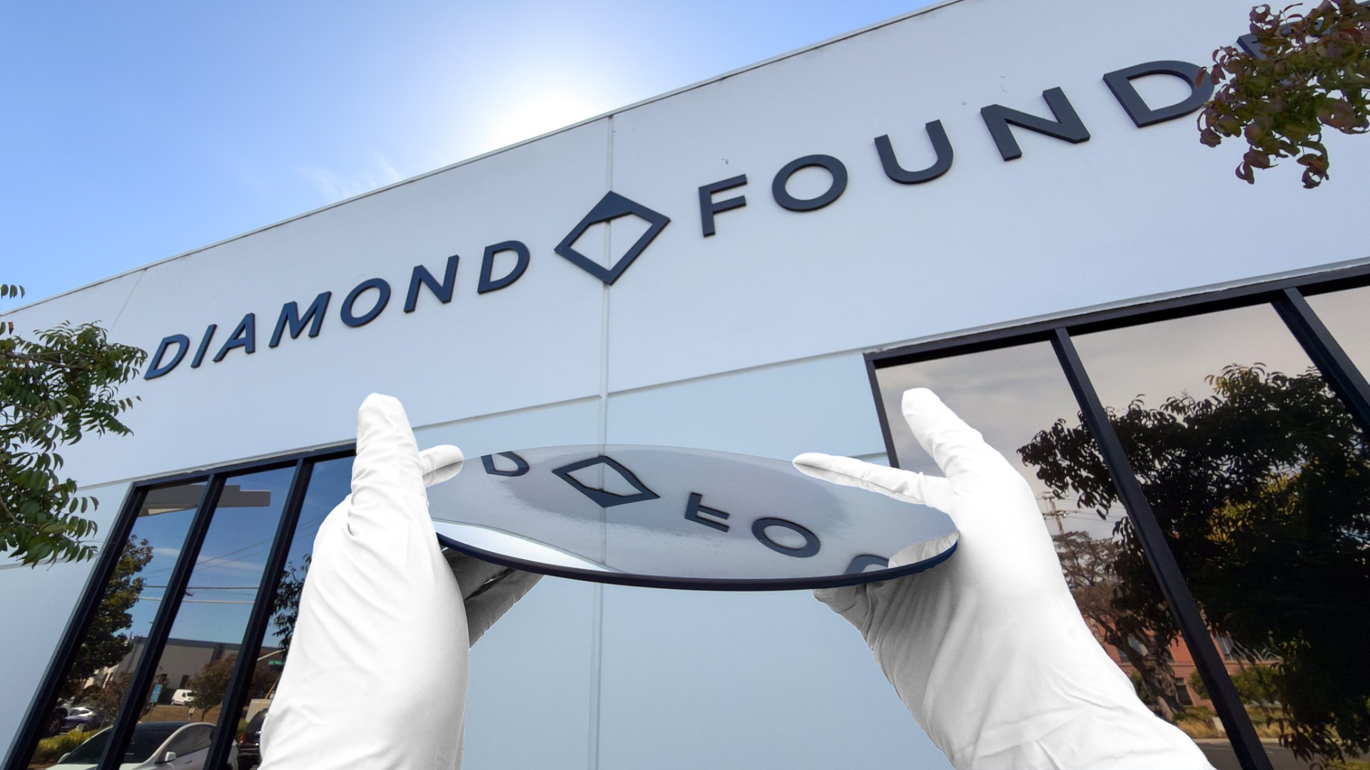
Addressing the historical scalability barrier of synthetic diamond production, Diamond Foundry has successfully fabricated the world's first 200mm single-crystal diamond (SCD) wafer. Unlike polycrystalline gem variants that suffer from grain-boundary phonon scattering, high-quality single-crystal structures preserve optimal lattice phonon transport, yielding extreme thermal diffusivity. Although the initial prototype currently exists in an unpolished state requiring downstream planarization and finishing processes, this development transitions diamond substrates from boutique laboratory specimens to standard wafer-scale semiconductor manufacturing dimensions, positioning the technology for potential 300mm roadmapping by 2030.
Empirical Benchmark Matrix
To contextualize the thermodynamic and geometric advantages of Diamond Foundry’s 200mm SCD wafer against traditional packaging and cooling methodologies, we evaluate key material parameters across competing industry implementations, including Akash Systems' GaN-on-diamond synthesis, De Beers Group's copper-diamond composites, and Frore Systems' diamond-infused liquid cooling cold plates.
| Substrate / Cooling Tech | Thermal Conductivity (W/m·K) | Max Wafer Format | Primary Application Vector | Electrical Properties |
|---|---|---|---|---|
| Pure Copper (Baseline) | ~385–400 | N/A (Bulk/Sheet) | Standard Heatsinks, Heatpipes | Conductive |
| Diamond Foundry SCD | ~2,000+ | 200mm (D200) | AI Chip Thermal Interposers | Dielectric / Insulating |
| Akash Systems GaN-on-Diamond | ~1,000+ | 150mm / Custom | RF Power Amps, High-Power GaN | Semi-Insulating |
| De Beers Cu-Diamond Composite | ~500–700 | Custom Blocks | HPC & AI Substrate Heat Spreaders | Hybrid / Tunable |
| Frore Diamond-Infused Cold Plate | ~1,500+ (Composite) | Liquid Plate | Nvidia Rubin / High-Draw GPUs | Isolated via Fluid Barrier |
Thermal, Efficiency & Definitive Verdict
The introduction of a 200mm single-crystal diamond wafer directly targets the localized current-density hotspots plaguing advanced-node silicon logic. By integrating SCD interposers or substrates directly beneath high-power compute dies, engineers can mitigate junction temperature spikes by upwards of 20°C, thereby unlocking substantial overclocking headroom and sustained frequency stability under heavy multi-threading. While fabrication cost, post-growth polishing yields, and epitaxial integration with silicon wafers present non-trivial engineering challenges, Diamond Foundry's achievement signals a paradigm shift. For next-generation high-performance computing and dense AI hardware clusters, single-crystal diamond is transitioning from an exotic anomaly to a mandatory structural component for thermal survival.